S100 Computers

Home S-100 Boards History New Boards Software Boards For Sale
Forum Other Web Sites Quiz Index    
  
An S-100 8086 CPU Board.
  
A number of the later S-100 board manufactures had their own 8086 CPU card.  Some had dual Z80/8088 CPU boards. There were even a few 8 bit 8088 S-100 CPU boards.  These boards moved the S-100 bus capabilities into the 16 bit world. Software was usually either CPM86 or a variation of MS-DOS.  This was at the time the IBM-PC and PC clones began to dominate the area and so IBM-PC compatibility became the rage. Few succeeded in true software/hardware compatibility. Only CompuPro or Lomas based board systems came close to achieving this goal.  One of my goals will be to do this.

I built a very early S-100 8086 prototype board back in the early 80's.  Here is a picture of that board:-

8086 Prototype Board
The board was configured in the 8086 "MAX" configuration so it could accommodate an Intel 8089 I/O coprocessor and Intel 8087 math coprocessor. The board (still) works well up to about 5Mhz in my system.  It runs fairly hot however with these old chips -- thus the heat sinks attached to each chip!  Because of space limitations there was no on board monitor EPROM. Instead the board booted directly from RAM/ROM on the S-100 bus at FFFFF0H.  BTW, this is where our Z80 CPU board with its ability to address 1MG of RAM came in real handy. Because one can easily deposit 8086 code at that area in RAM for board testing etc.  Considering the fact that this was a 3 chip set, it has remarkably few IC to work in an S-100 system. This is to some extent due to the fact that the S-100 bus is really geared to an Intel type of hardware system.  The board turned out to be very reliable and allowed me to develop much 8086 software. I installed both CPM86, the unofficial upgrade CPM86+ and MSDOS using this board. 

However I felt any new S-100 8086 board should be capable of running at a higher speed, something in the range of 8MHz using the later 8MHz chips.  Consequently I modified the above board fairly extensively.   I decided not to include the two coprocessors. I reasoned that anybody needing this capability will be using an 80286 or 80386 S-100 board (future boards, later this year).  Instead I decided to place an onboard pair of EPROMS on the board.  Using the schematic shown here, Andrew and I drew up the following early prototype. Here is a picture of that board:-

8086 V2 Prototype

Here is a schematic for this board.  There are more support chips on this board because we are now including the two EEPROMS. As we shall see below these two chips require their own address and data buffers (5 chips).

BTW, if you wish to understand the 8086 CPU in detail an outstanding source of information is the Osborne/McGraw-Hill 1980 book: "The 8086 Book" by Russell Rector & George Alexy. The Intel Data sheet can be seen here.

Let us look at the boards components one at a time. 
 
The Master/Slave Transfer Logic
This board upon power on or reset will normally exist on the S-100 bus as a slave CPU board. That is it will be inactive while the Master CPU (usually a Z80) board is active. (It can be configured as a Master itself, but lets pass on this for now).   Please look at this diagram.
   

Reset Circuit
   
As setup the Intel 8284 "Clock Controller" holds the 8086 in a permanent reset state (pin 11 is low).  The S-100 bus allows for up to 16 slaves (CPU/DMA) boards. They are selected by the four S-100 lines TMA0-3 (pins 55-57 & 14).  I will use the TMS0 line here.  To activate the board we lower TMA0 (typically by outputting a bit from a port elsewhere on the bus, e.g. the SMB, but this could even be a bounce less switch).  This lowered signal is passed along step by step the three 74LS74 flip flops A,B & C. A and C are clocked by the S-100 bus master clock Phi.  The output from flip flop A is sent back to the bus as a low on the S-100 line HOLD* (pin 74). This tells the Z80 another board wants the bus. When it is ready it raises the S-100 hold line pHLDA which clocks the flip flop B. This is then clocked (by Phi) through flip flop C and eventually raises the Res* pin 11 on the 8284. This releases the 8086 from its reset state. The output of flip flop B also puts out the important signal XFERII which amongst other things allows the "new" Phi clock signal for the 8086 to appear on the bus.  Meanwhile at this time all the Z80 status, data, address and control lines are tri-stated.  It's as if the Z80 no longer exists on the bus.

Now it should be pointed out that the original IEEE-696 specs allow for only 1 master clock on the bus. In real world practical systems this usually meant the Z80 clock.  It was not long however until almost every S-100 board manufacture  adapted a modification (like that above) that allowed the slave CPU to supply its own (faster) clock.  This is what I will use in all our Slave S-100 boards.  It is important also to remember that this board cannot itself transfer control to another slave board (for example a DMA controller) the board/software must refer back to the true S-100 bus master.  This is how the IEEE-696 protocol was setup.

Intel allowed two sources for the actual clock frequency generation. A crystal connecting to pins 17 & 17 of the 8284 or a clock oscillator connected to pin 14. Pin 13 determined the source.  In both cases the input frequency is 3X the desired output frequency.   For flexibility, I allow both sources to be used. I started with a 24Mhz crystal.

Status and Control Lines
It is absolutely critical that the above transition takes place in an orderly fashion where at no time are any of the S-100 bus lines left floating -- no matter how short the time.  This is accomplished in a two step process called XFERI and XFERII.  In XFERI the Z80 bus status, data and address lines are switched over to the 8086 but the Z80 still retains control of the critical control lines pSYNC, pWR*, pDBIN and pSTVAL*.   In this way even though all the other S-100 lines are getting switched over nothing will happen to any of the S-100 boards (if they are IEEE-696 compatible).   No memory will be written to with garbage, no ports accessed etc.  When that transfer is complete, only then, does the second XFERII process take place.  For a very brief period of time the Z80 and 8086 will BOTH be controlling the pSYNC, pWR*, pDBIN and pSTVAL* lines.  (That is why on well designed boards they have 10 Ohms resistors -- to protect the bus drivers).   Once the Z80 signs off (one Phi clock cycle later), the 8086 has complete control of the S-100 bus.
    
Control Lines
  

This whole process seems complicate at first and to some extent is,  but a lot of thought, care and attention was put into it by the original IEEE-696 committee to allow for an extremely reliable system.

If you don't quite understand the above, don't worry just look upon the circuits as a "black box" for Master/Slave switching. 

The actual generation of the critical 8086 control signals is relatively straightforward. Intel did a good job of presenting a simple symmetrical set of signals. First look at the following diagram:-

Control Generation

First it should be stated that  the 8086 actually can be configured in two different configurations. A "MIN" and a "MAX" mode depending on the status of pin 33. If pin 33 is high the 8086 configures itself in the MIN mode. This configuration is meant for simple 8086 applications where there is a minimal (if any) bus structure and no co-processor support.  The memory and port control lines come directly from the CPU.  The MAX mode is different (pin 33 to ground),  in this case the 8086 configures itself for a multi-processor arrangement with a bus structure and possibly co-processors.   The control lines do NOT come directly from the CPU but instead three lines S0, S1 and S2 send encoded information to a special "Bus Controller" called an 8288, (see here for specs).  This chip interprets the S0-S2 signals and puts out the appropriate Memory/Port RD/WR signals.  The interpretation is fairly straightforward and can be summarized as follows:-

S0-S2 Table

As you can see we have all the raw information we need to generate the S-100 bus signals.  All we have to do is construct a pSync and pSTVAL signal.  In fact a simple 74LS138 will get you a similar set of signals. We could in fact do away with the 8288 entirely except for the fact that that chip  does put out a special "Advanced" memory write control and "Advanced" I/O control that allows the system get an earlier signal than would be available with S0-S2 alone. This give us more memory and I/O access times.  This alone would probably not be a reason enough for adding this extra chip. I use it because as we shall see when we later move up to a 80286 board we will absolutely need a bus controller chip. May as well get the bugs worked out on a simpler system!  Nevertheless I do use a 74LS138 (U67) to control an LED bar at the top of the board.  The LED's in the bar (left to right) individually signal when the 8086 state is:- INTA, I/O-IN,  I/O-OUT, HALT, an M1 Cycle, MEM-READ,  MEN-WRITE, and PASSIVE.  These are quite useful when you single step the CPU in the S-100 Bus.

The outputs of the 8288 are combined to yield the appropriate S-100 signals and placed on the bus via U56.

Data and Address  Lines
The 8086 multiplexes its 20 address lines and 16 data lines. Both come from the same set of pins on the CPU.   This complicates things slightly. For each bus cycle the address lines are first presented. They must be latched into the Intel 8282's (U73,U74 & U75) with the ALE (Address Latch Enable) from pin 5 of the Bus Controller (the 8288).  Only later does the DEN (Data Enable, pin 16) signal appear which activates the S-100 data bus drivers, Intel 8286's (U76 & U77).  The Bus Controller signal DT/R (pin 4) determines the direction in which the data flow is expected (to the CPU or to the S-100 Bus).
Here is a summary of the layout:-

Address Lines

This two step multiplexing of address and data slows the 8086 down and was done away with in the later 80286 chip.  Nevertheless when done properly it is very reliable.

All this would be fairly straightforward if it was not for the fact that the 8086 will input and output either 8 or 16 bits of data.  The special sXTRQ* of the S-100 bus must be handled to let other boards on the bus know what to expect.   I have discussed at length elsewhere on this site this process. See here.  Fortunately the 8086 has a special pin BHE (Bus High Enable) which greatly simplifies this process. Pin 16 of U84 delivers sXTRQ*  to the S-100 bus.  

The 74LS244, U78, takes care of the transferring both memory and port ODD address IN  8 bit data (or interrupt return vectors - typically from an 8259, see here) to the lower byte data bits of the 8086 where it expects to find them.  The circuitry took quite some time to figure out and for most is best looked upon as a "black box".


The Onboard EEPROM  
As I said above, my original prototype board did not have an onboard ROM.  Instead after a reset it looked at the S-100 bus RAM at FFFF0H.  There are some advantages to this. With a Z80 system that can examine and modify RAM at this location (see here) you can quickly test a board. This will be described below in detail.  However there are advantages to having a powerful on-board EPROM monitor on the board -- particularly if it is to be a bus master and the only CPU in a system.

Unfortunately adding an EPROM takes more space than you might expect.  In order to simplify the hardware, first we use two EEPROMS, a high and low byte.  This avoids the need for a BHE pin function since the 8086 will never be a write to this memory location,  (the CPU itself takes care of the data lines for High/low input data). However we do need to latch the address lines as we do for the "normal" S-100 address lines. Furthermore whenever the 8086 is addressing the onboard EEPROM it must inactivate completely the drivers to the actual S-100 bus.   The EPROM_SEL* signal generated as shown in this schematic does this:
  
EEPROM Circuit
   
Note how the outputs from the data pins of the two EEPROMS directly drive the data pins of the 8086 once ROMRD* is low.  Note also how EPROM_SEL* inactivates the S-100 drivers in the above previous schematic.  With SW3 the EEPROM can be configured to many different sizes, we will typically take up only the top 64K of the 8086's 1M address space.


A FINAL PROTOTYPE 8086 BOARD
Much was learned from the above board.  It worked very reliably at 6MHz but was unreliable above that.  Andrew and I went through two further prototype boards to arrive at this final prototype board which we are quite happy with.

V3 Prototype
Most of the changes are minor and subtle. I will not spend much time recalling some frustrating experiences tracking down bugs.  The schematic of the final board can be see here.  Amongst the changes were:-

  Switched bus drivers from Intel 8282's & 8686's to the more common (and far less expensive), 74LS373's and 74LS245's.
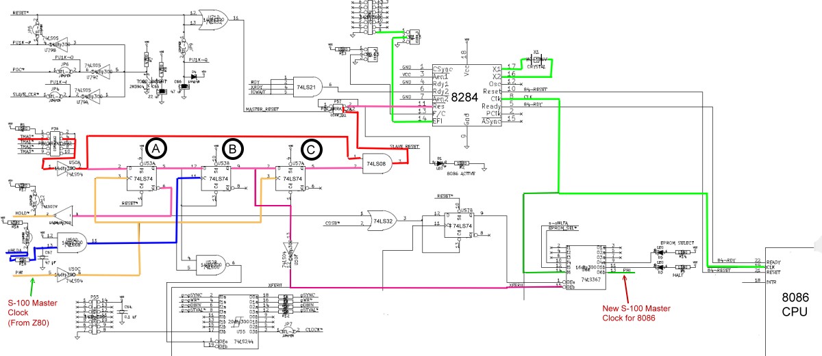
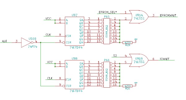
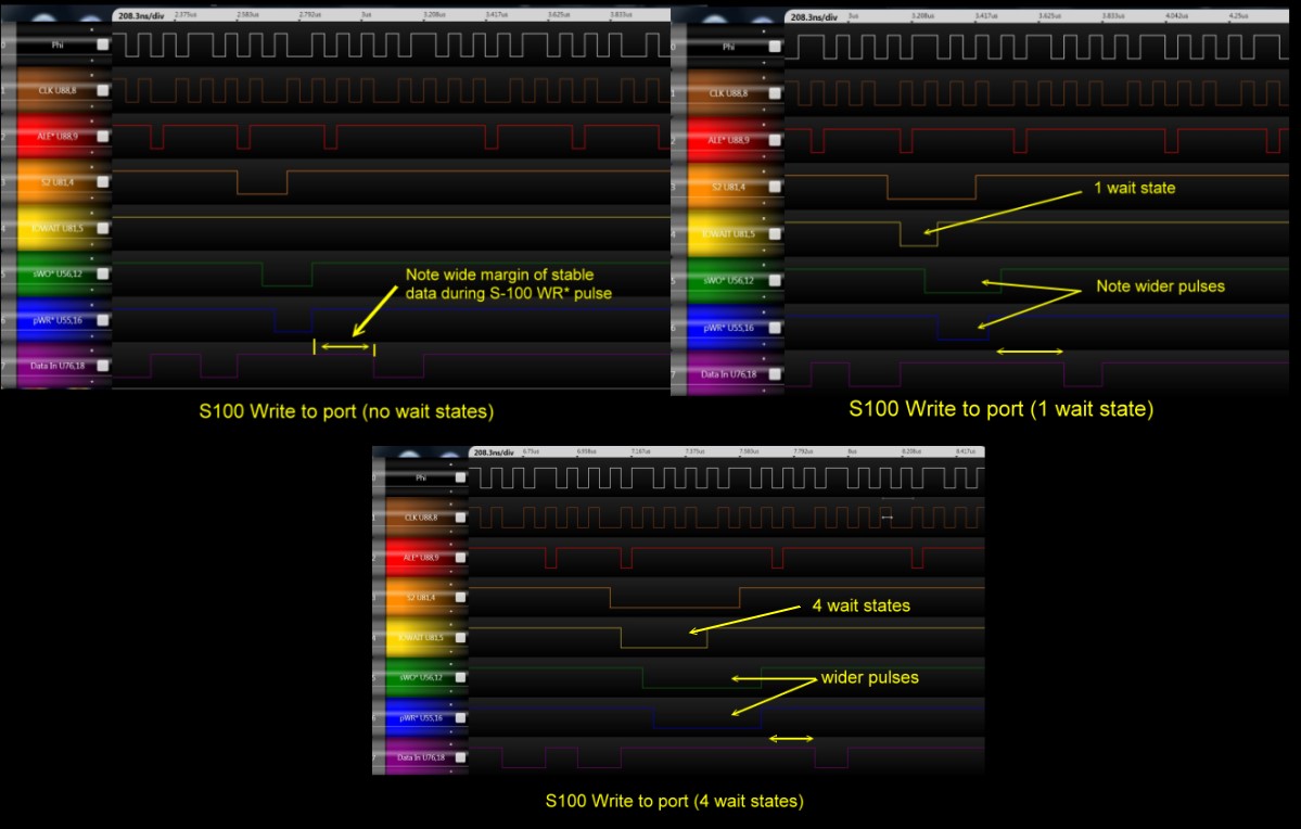
  Completely redid the wait state circuitry (allowing 0 to 8 weight states) for slow old  I/O boards and the onboard EEPROM/ROMs
  Adding on the board an IO port board circuitry that allows any CPU to switch on the board (no longer need the SMB or an external switch).
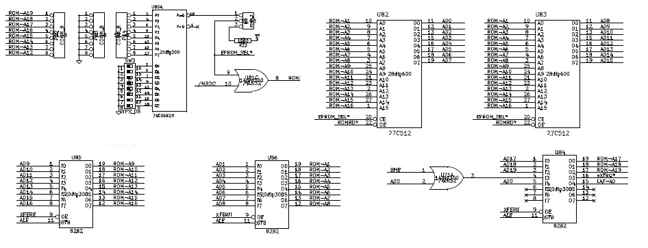
  The board can now utilize either 27C512 (or more practically) 28C64 EEPROMS
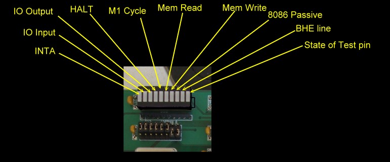
  More LED's to show what is going on.

The board in my hands will work (at 8MHz - see below) with any of the S100Computers/N8VEM  we made over the years. It also works with a number of IEEE-696 Memory boards such as the CompuPro 128K static RAM-21 board, the 256K static RAM boards from BG Computers or Fulcrum and the Electrologics 1MG Memory Disk.  I have not tested it with any Dynamic RAM boards. If these boards have their own onboard refresh controller I suspect they would be fine -- at least up to 6MHz.   If however they rely on the Z80 refresh signal (non-IEEE 696 boards), they defiantly will not work.

For the board to run at 8MHz it has to be jumpered for (at least) two wait states for I/O in order to utilize I/O ports on other S-100 boards. Also for reliability a number of the 74LSxx chips need to be changed to the faster 74Fxx types.  These are indicated in the schematic. The Achilles heel of the board is for fast 8 bit reads of memory from odd address lines. The S-100 bus brings this 8 bits of data in to the board on the upper 8 bit (S-100) data lines.  They must be shifted down to the lower 8 bit data bus via U78 and then passed through U75.  This unfortunate "in, across, and then in"  process has a slight timing overhead, so it is important that the logic involved is fast. Thus the use of 74Fxx chips in these areas (U52, U60, U72, U58, U71, U78) on the board.

Realizing that people may wish to use this board with old S-100 boards that have slow I/O access times (old IMASI/Altair 2MHz systems) I added the following circuit that allows up to 8 wait states to be inserted during any S-100 bus Port I/O.

Wait State Circuit

The IOWAIT line feeds into the RDY line of the 8284 clock generator.

Here are some logic signals on from the board with 0,1 and 8 Wait states:-

Wait States

BTW, don't worry about the irregular top clock pulses. The reason they vary a little is because the data access rate of the PC based logic analyzer cannot keep up fast enough. The data analyzer gave the WR* pulse width at 8MHz with 0-4 wait states as:-

0 = 125 ns, 1 = 208 ns,  2 = 291 ns, 3 = 375 ns, 4 = 416 ns

With this board you can go up to 8 wait states! More than 4 however is probably not practical.

The board can be "single stepped" on the S-100 bus using for example our SMB board.  It is important to remember however that the 8086 has an internal 6 byte "look ahead" queue, so the status signals on the bus actually are slightly ahead of what the 8086 internally is doing. Normally this is not seen -- unless the queue is jumped by an opcode like JMP.  The 10 panel LED Bar at the top of the board indicate the current 8086 cycle.  Here is the breakdown:-

LED Bar
If you put the following code in RAM at FFFF0H:-

B0, 33, E6, 01, EB, FA

and jump to it (reset point for 8086), The 8086 will continuously out the ASCII latter '3" on the console port 1. If you have the S100 Computers/N8VEM SMB and single step the 8086 you will see the appropriate LED's come on as indicated above.

The fourth from the left LED bar is useful as we shall see in building the board. If you fill a ROM with 8086 "HALT" instructions (F4H). It should be the only bar lighting up if the 8086 reads RAM/ROM correctly. This test is independent of any even/odd 8 or 16 bit logic on the board.

The board will work with older 8086's (and 8284's & 8288's) at 6MHz.  To reach 8MHz you need the equivalent chips. The 8MHz Intel chip is called 8086-2.  However these Intel chips do run hot. It does not seem to bother them, but I always like to run cool boards in my system. Consequently I normally use the CMOS equivalent chips. I use the NEC V30 chip. This is a completely hardware equivalent CMOS chip to the Intel 8086 and is in fact rated for up to 16MHz!.  I use the CMOS equivalent 82C84 and 82C88 support chips as well.  These run almost cold. The boards Voltage regulator is only warm.  A good source of these chips is Unicorn Electronics.  The V30 is harder to find, though they are usually on eBay. I got mine from a friend.


Step By Step Building The Board.
Since for many this board may be their first venture into putting a 16 bit system in their S-100 bus I will go into some detail as to how to get it up and running.  There are 3 simple pieces of 8086 code that are your best friend! 

HALT's.

Whenever the 8086 sees a halt instruction (a single byte F4H) in RAM/ROM it will stop everything and remain there until reset.   So the first thing we will do when we put together the board is have it see memory with just F4H's.  It must halt. The above 3rd from left LED bar must come on (as well as the special HALT LED D3).  This process is independent of any Odd/Even address or in fact any RAM/ROM location.   You must get this working before going further.


(B0, 33, E6, 01, EB, FA)
START:  MOV    AL,33H
              OUT    01H,AL
              JMP     START


You will typically place this code at FFFF0H in RAM or ROM.  This the start reset address of the 8086 at the very top of its 1MG address space. This code is position independent but does require a functional Odd/Even address circuit to work. If all is well you will see continuous letter "3" on your console (assuming it is at port 1H). 

Now there are a number of ways you can get this code setup before the 8086 sees it.  First, it's way outside the Z80 CPU's 64K address space.  So if you wish to place it in RAM at that location (using for example the 4MG static RAM Board) you need a CPU board that can address a window in a 1MG address space.  Our Z80 CPU board does this easy. As does the Intersystem's Z80 Series-II  board.  Here are the keyboard commands for the former CPU board:-

QO D2, FC                               ;Temporally allow the Z80 to access RAM at FC000-FFFFFH at 0-3FFFH
S3FF0  B0,33,E6,01EB,FA         ;Insert the above code at FFFF0 in RAM
QI ED                                      ;Inputting port ED activates the 8086.

The advantage of this approach is you don't have to burn any 16 bit pairs of ROM's.  The memory board (if its IEEE-696 compatible), will take care of the odd/even byte addressing for you.        


Alternatively you can burn the above code in a ROM or EEPROM. Using either the onboard ROM sockets or an external EPROM board (again if its IEEE-696 compatible) such as our one here.  There is one catch however. You have to burn two separate PROMs. One with the even set of bytes, the other with the odd set of bytes. These PROMS are labeled "H" and "L".   Now for a short piece of code like we have here you can probably do this by hand.  However as we will see in the software section for more elaborate code you need to have software that will do this for you.  Fortunately most EPROM programmers have this option. I really like the Weldon VP-280 type programmers. They are Windows 7 compatible and very easy to use. See here.

Again inputting port ED will activate the 8086 where it will pick up the above code in the EEPROM.

(EA 00 05 00 00)
         JMPF      500H
This code which we place at the 8086 reset address (FFFF0H) causes the CPU to immediately jump down to 500H in RAM.   Here we can place any code we like. Start with the above B0,33,E6... code.   This will test your boards ability to read RAM reliably.  This BTW is where we will place the CPM86+ boot code.  If you get this latter piece of code working you are well on your way of having a hardware functional S-100 8086 board.

I will provide the usual step by step build instructions for this board when new bare boards arrive. Stay tuned!

Bringing up an 8086 Monitor and CPM86+ in an S-100 System.
To be of any use we clearly need a disk operating system to work with this board.  There are really two options: CPM86 or some type of MS-DOS. I have used both in the past .  However again realizing this may be a dramatic step for people coming from the 8 bit world, I will start with a 8086 Monitor for the onboard EEPROMS and then "do" CPM86+.  Please click here to get to the 8086 Monitor software section of this web site for the 8086 Monitor details,  or the CPM86+ section for step by step instructions about bringing up CPM86+ on a CPM(80) system for the first time. 

Link to 8086 Monitor and Video Describing the Board.
Link to CPM86+

A Production S-100 Board.
Realizing that a number of people might want to utilize a board like this, together with Andrew Lynch at N8VEM (see here) we are collecting the names of people that would like such a board. If you have an interest in such a bare board, let Andrew know via e-mail at:-  lynchaj@yahoo.com
 
Please note all the above clearly applies only to people who know what they are doing and can  do a little soldering and board assembly.  There will be little hand holding at this stage.  This board (and defiantly related software) is more complicated than some of the other boards on this site.

The links below will contain the most recent schematic of this board.
Note, it may change over time and some IC part or pin numbers may not correlate exactly with the text in the article above.

MOST CURRENT 8086 CPU BOARD SCHEMATIC  (V3, FINAL, 06/19/2010)
MOST CURRENT 8086 CPU  BOARD LAYOUT  (V3, FINAL, 06/19/2010)


Other pages describing my S-100 hardware and software.
Please click here to continue...

This page was last modified on 09/18/2011